 |
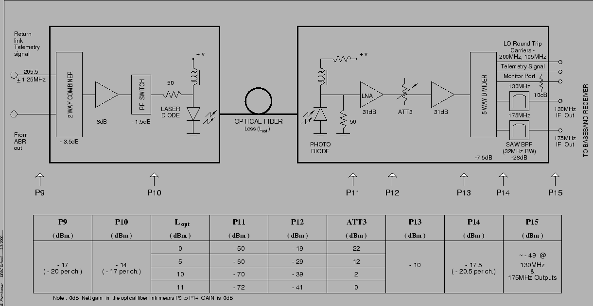
Figure 21.5 shows the schematic block diagram and the nominal powers at different stages of the the fiber-optic return link21.14. The link consists of a laser diode (which converts the input electrical signal into an optical signal), the optical fiber itself, a photo diode (which converts the optical signal back into an electrical signal) followed by an amplifier and a 5 way divider which separates out the monitoring data as well as the two polarizations of the astronomical signal.
The Fiber optic link is designed to provide a net gain of
0 dB from the input (P9 in Figure 21.4) to the output
(P14 in Figure 21.5) which is also the input to the
baseband system discussed in Chapter 23. The
link is meant to have 0 dB gain irrespective of the length of
the fiber optic
cable linking the antenna to the CEB. The attenuator (ATT3 in the
Figure 21.5) can be varied in accordance with link
optical loss to provide this no loss/gain configuration. The level
diagram shows the attenuator settings for 0, 5, 10 and 11 dB
of optical loss (L![]() ).
).
The fiber-optic receiver also contains 32 MHz SAW filters
centered at 130 and 175 MHz to separate out the 130 and the
175 MHz IF signals for routing to the base band converter subsystem.
The level of the signal at this point (P15) is nominally
![]() dBm21.15
dBm21.15
 |
 |
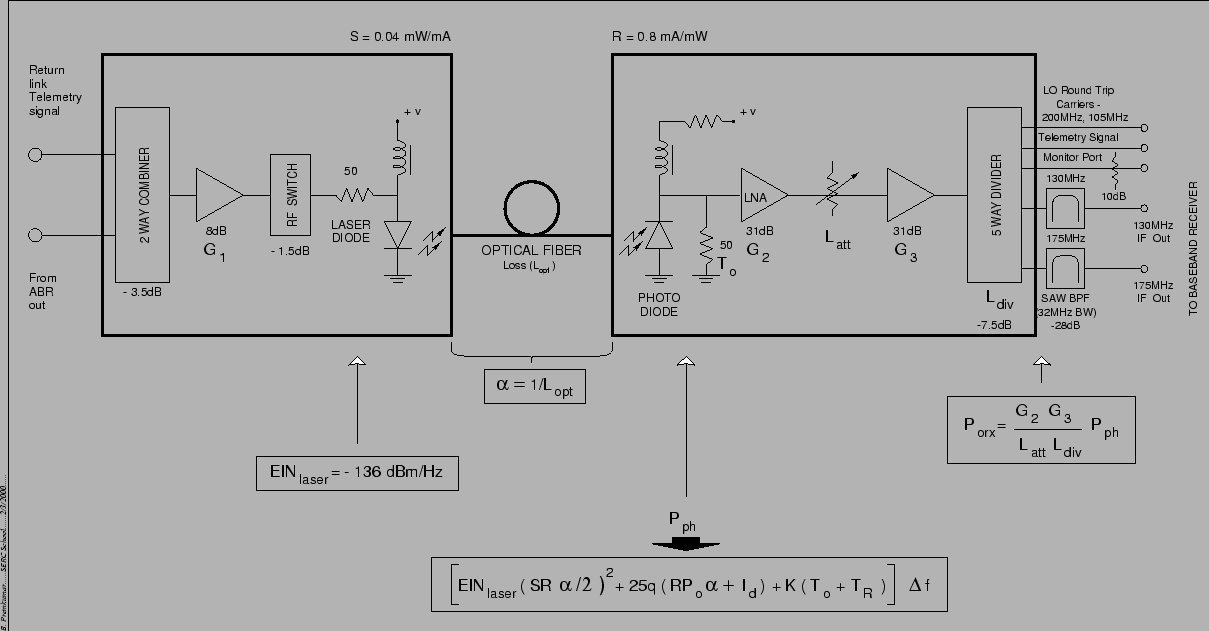
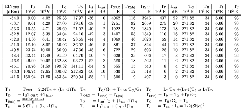
An ideal communications link would transfer signals unaltered
from the input to the output. Any real link however introduces both
additional noise as well as distortions into the signal it transports.
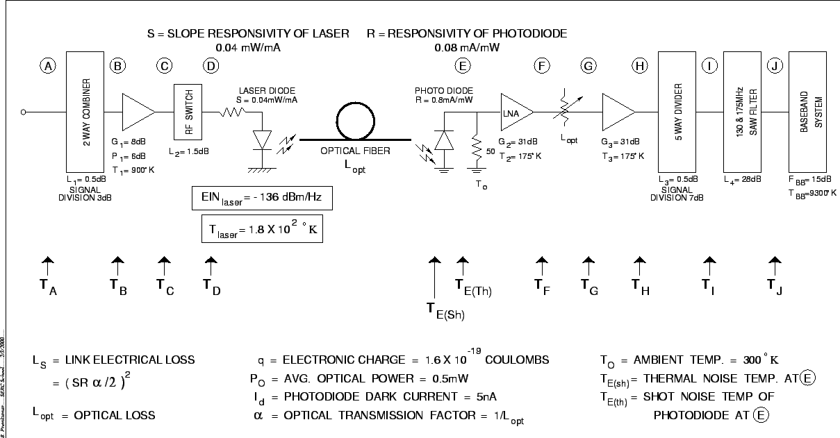
In the GMRT fiber-optic link, these non idealities include the
laser intensity noise, shot noise and thermal noise of the laser
diode, loss and reflections in the optical fiber, as well as shot
noise and thermal noise in the photo-diode. Figure 21.6
gives expressions for these various noise terms, and Figure 21.7
and Table 21.7 give the expected values for the various
noise terms for the GMRT fiber optical link. The largest loss is
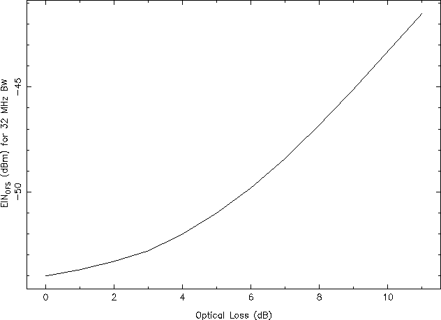
for the most distant antennas, and turns out to be ![]() dB.
From Table 21.2 (or Fig 21.8) the corresponding
equivalent input noise (EIN) is
dB.
From Table 21.2 (or Fig 21.8) the corresponding
equivalent input noise (EIN) is ![]() dBm. The nominal input
power level (P9) of
dBm. The nominal input
power level (P9) of ![]() dBm would hence give a signal to noise
ratio of
dBm would hence give a signal to noise
ratio of ![]() dB, i.e.
dB, i.e. ![]() . In this case, the system temperature
is degraded by 1% due to noise added by the link.
. In this case, the system temperature
is degraded by 1% due to noise added by the link.
 |
 |