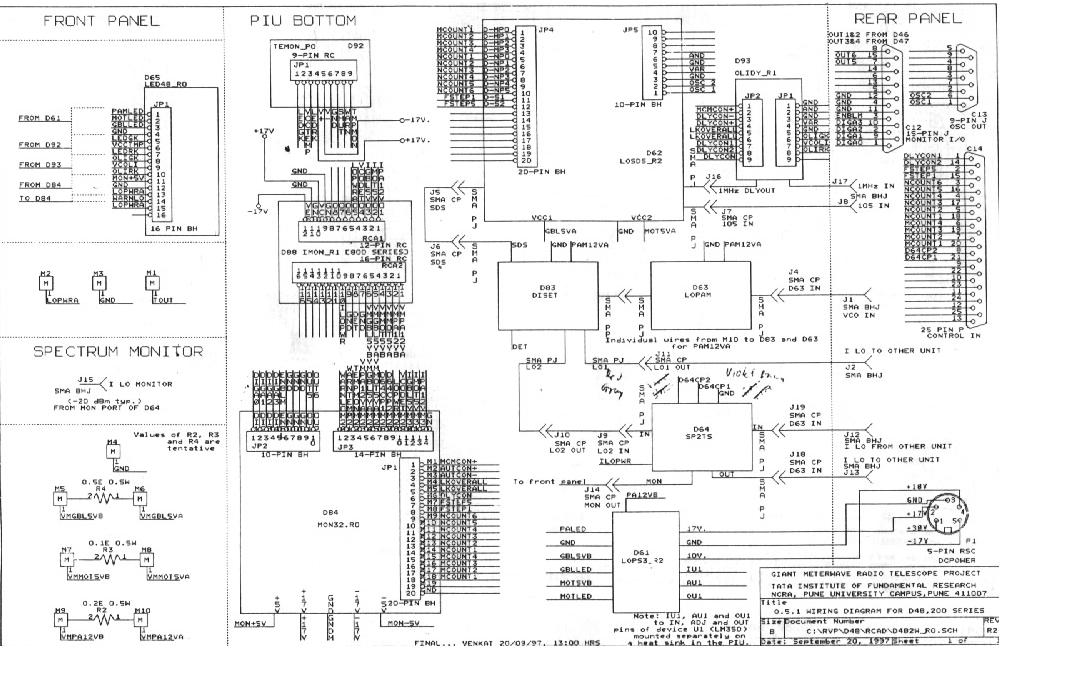
LO System
LO synthesizer 2
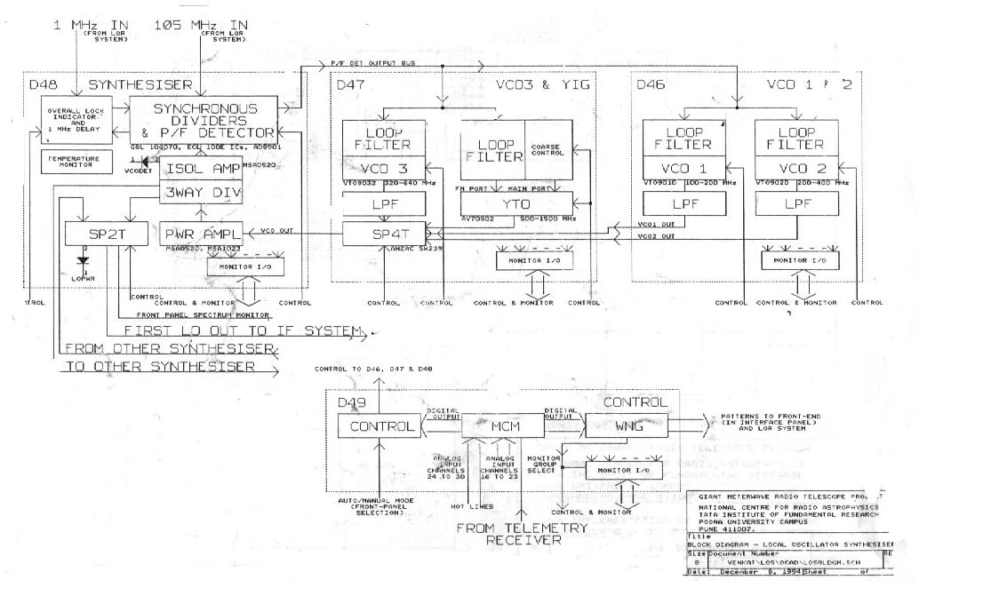
- Block Diagram
- VCO 3 and YIG
- Block Diagram
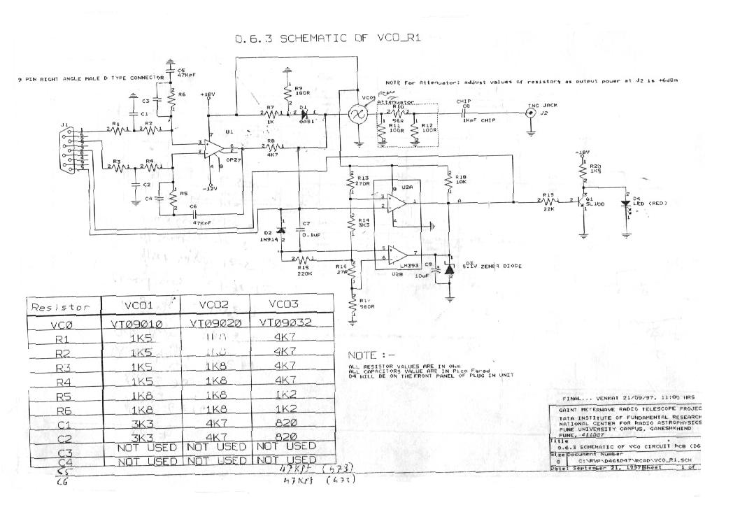
- Voltage Controlled Oscillator 3
The Voltage Controlled Oscillator 3 (VCO3) is used in the D47 PIU and is a part of the LO Synthesizer 1.
The range of working for oscillator is predefined and is 400MHz to 600MHz with a step size of 5MHz.
There is a "guaranteed range of operation" for the oscillator typically from 10% to 90% of the range of oscillator specified. For VCO 1 the range of operation is from 325MHz to 680MHz without any hitch.
The DC supply given to the oscillator is given through MCM-controlled Relays. The DC power to the oscillator is switched off when not in use to eliminate any chance of system produced spurious signal affecting the receiver performance.
The VCO 3 is favored to VCO 2 for synthesizing the frequencies in the range 320 to 400 MHz as the prior operates at lesser control voltage than VCO 2.
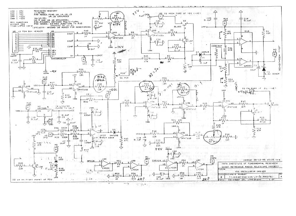
- YIG
The YIG stands for Yttrium-Iron-Garnet. The YIG is used in D47 PIU and is a part of Synthesizer 2. The range of working for oscillator is predefined and is 400MHz to 600MHz with a step size of 5MHz. There is a "guaranteed range of operation" for the oscillator typically from 10% to 90% of the range of oscillator specified. For VCO 1 the range of operation is from 450MHz to 1795MHz without any hitch.
The DC supply given to the oscillator is given through MCM-controlled Relays. The DC power to the oscillator is switched off when not in use to eliminate any chance of system produced spurious signal affecting the receiver performance.
- YIG Oscillator Driver
The DAC and OP 471 produces a linearly varying main port voltage based on the 8-bit digital input to DAC. Control is done using bits 1 to 6 of Address group 2. This is processed in the succeeding driver stage, with the setting of resistors determining the offset and the slope respectively of the transfer function. The circuit produces a current drive, varying from ~0 to 125mA, with a slope of around 2mA/YIGDAC bit. This causes the YIG coarse frequency to change by about 25MHz/YIGDAC bit.
The Control Voltage is processed in succeeding driver stage, with a R41 determining the offset of the transfer function. The circuit produces a current drive of around 40mV/volt which in turn causes the YIG frequency to change by around 8MHz/volt.
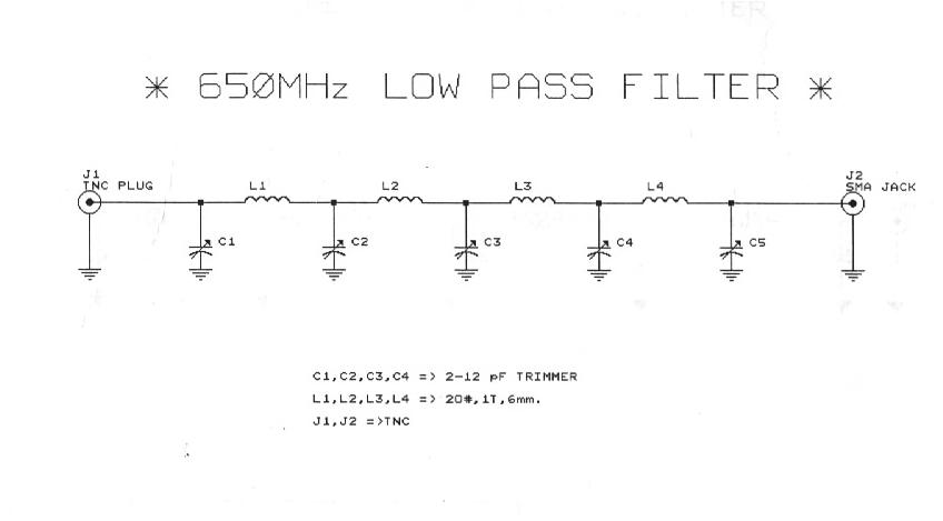
- 650 MHz Low Pass Filter
The 650 MHz Low Pass Filter acts as a frequency selective network which passes all the frequencies below its high cut off level. Some of the important characteristics are enlisted below.
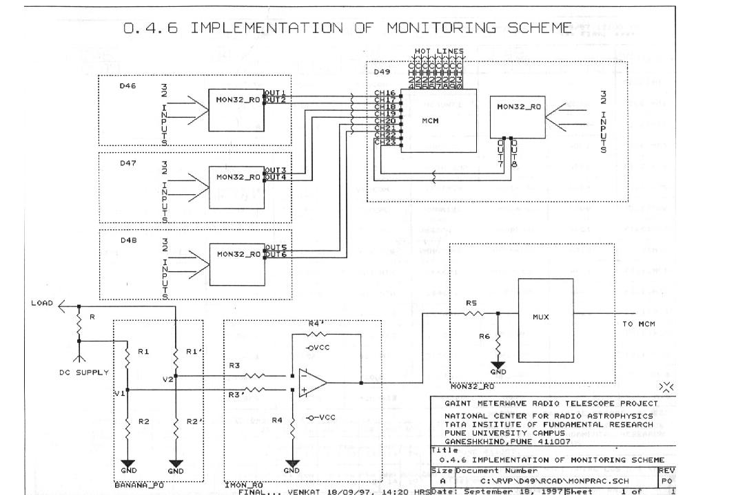
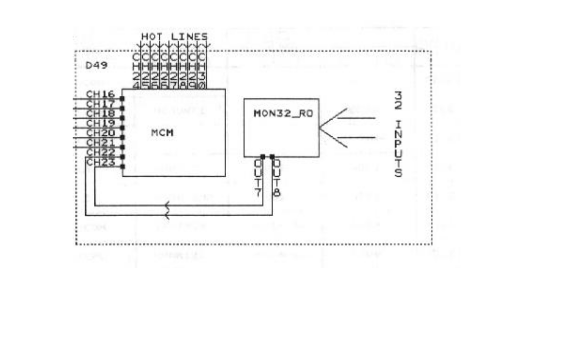
- Monitor Multiplexer
The Monitor Multiplexer acts as a 32:2 multiplexer. - Single Pole Four Throw (SP4T)
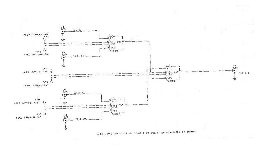
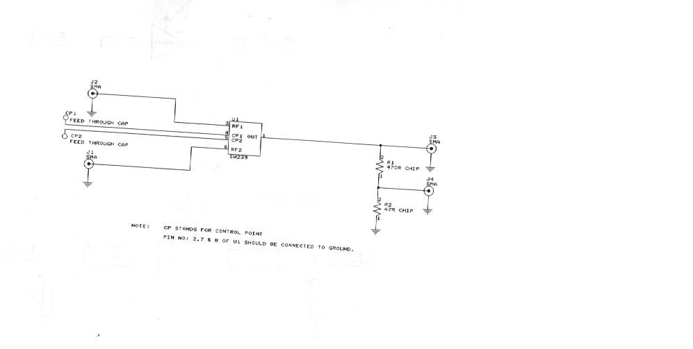
The single pole four throw chassis is used in D47 PIU. The chassis is designed by using three broad band RF switch. The RF switch uses SW239 to realize the function.
This is used to select any one of the four active oscillator for further amplification in the power amplifier in D48 PIU
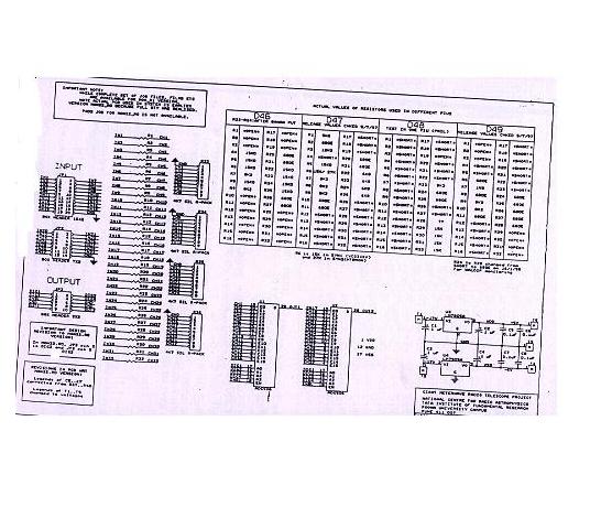
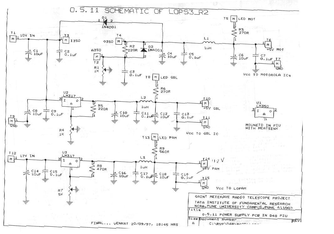
- Power Supply
The power supply is made up of an AC distribution panel and a DC distribution panel and both are employed for different purposes.
- Synthesizer
- Block Diagram
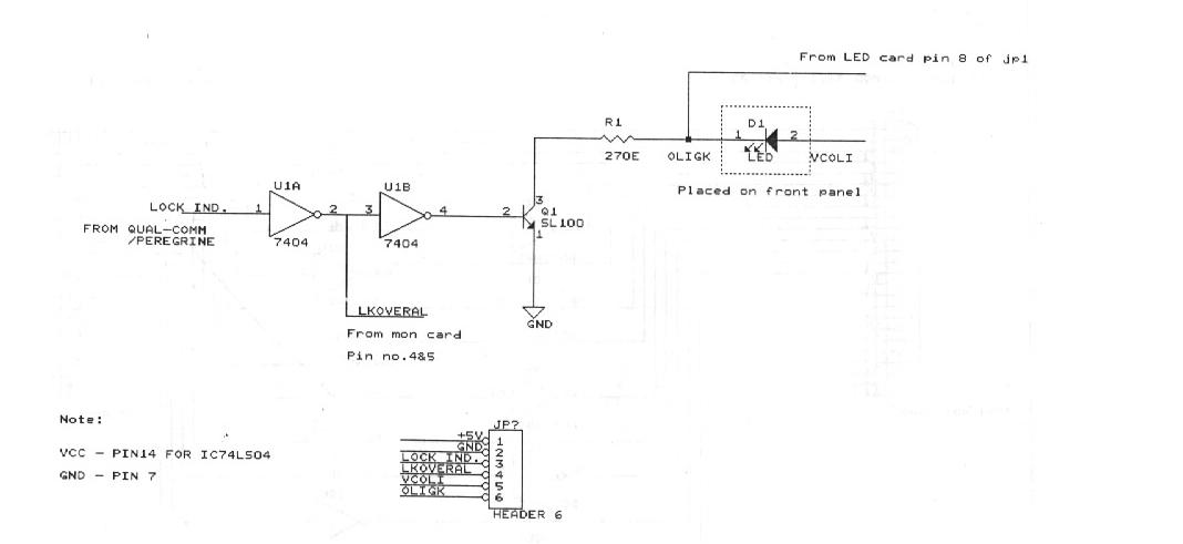
- Overall Lock Indicator
The Overall Lock Indicator is used to recognize the phase locking of the signal. The AD9696(U1 and U2) convert ECL output of reference and VCO-divided signals from the prescalar and the PFD module( at a frequency equal to step size, under lock) into TTL levels.
The monostable 74LS123 helps in a visual indication of the presence of these signals and helps in easy fault diagnosis.
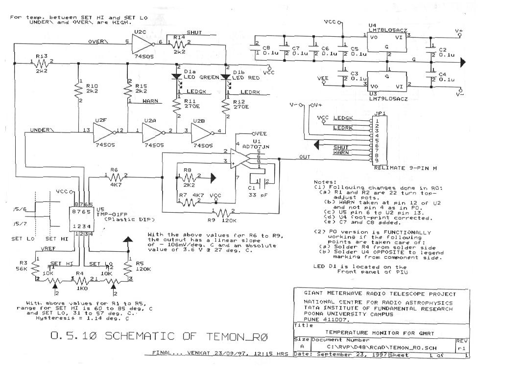
- Temperature Monitor :
The circuit is designed around Analog Device which provides an analog voltage of 5mV/degree K. It has got set of points, which could be used for WARN and SHUT purposes. Hysteresis has been provided in the IC to avoid jitter conditions at the set points.
- Qualcomm Prescalar
The Qualcomm Prescalar is backwards compatible with Q3236 PLL Chips. The phase noise contributions of the unit is as low as 154 dBc/Hz at 100 Hz from Carrier. The nominal power consumption less than0.6 W.The power supply +5 V is needed of the operation. It has wide input sensitivity range from -10 to +3.5 dBm. The 100 MHz Phase/Frequency Detector is included in this, which is a high gain linearized Phase/Frequency Detector with No Dead Zone as 302 mV/Rad. It is provided with a Out-of-Lock Indication facility.It can be programmed for Faster Multiplexing between Two Pre-loaded Frequencies.
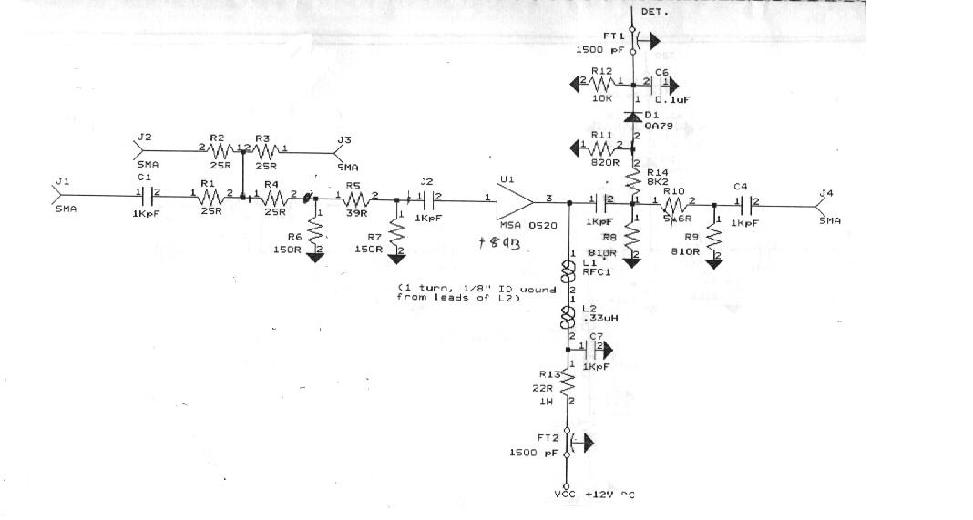
- Isolated Amplifier
The Isolated Amplifier is kept into a single chassis along with a power divider and a Detector. The Isolation Amplifier is a stage of Avantek MSA 0520 (Cascadable Silicon Bipolar Amplifier) modamp preceded by suitable attenuators. The Circuit initially divides the power coming from the Power Amplifier in D48 PIU into three parts. One of them acts as a First LO Signal to the mixer in the IF system.The other ones are to be given to the Isolated Amplifier stage and the output of the Isolated Amplifier stage is given to to the dual modulus prescalar.
The Isolation Amplifier stage helps in reducing the reverse leakage components from a prescalar to the first LO port to the acceptable level.
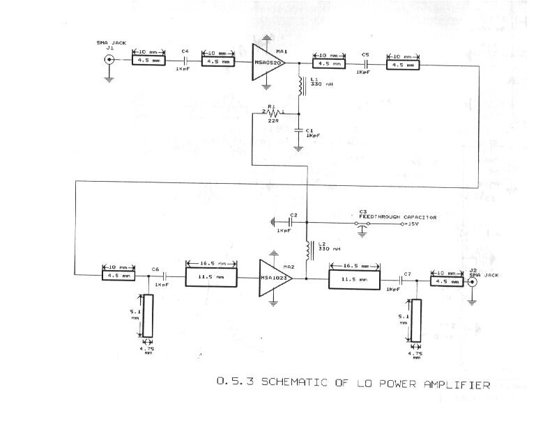
- Power Amplifier
The power amplifier amplifies the oscillator power input from around +5dBm to around +21dBm. The operating voltage of the unit is +12 V.
The unit is actually a cascaded 2-stage modular amplifier and uses MSA 0520 and MSA 1023.
- Single Pole Double Throw (SP2T)
The single pole Double throw chassis is used in D47 PIU. The chassis is designed by using single broad band RF switch. The RF switch uses SW239 to realize the function.
This is used to select any one of the four active oscillator for further amplification in the power amplifier in D48 PIU.
- Power Supply
The power supply is made up of an AC distribution panel and a DC distribution panel and both are employed for different purposes.
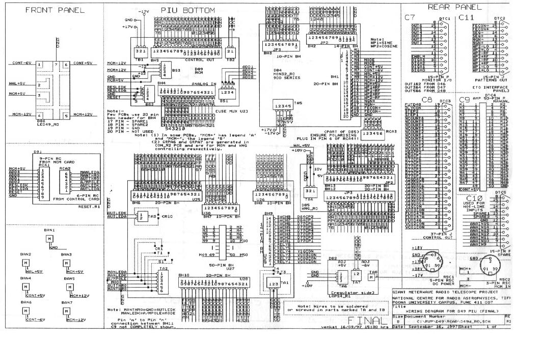
- D49 - Control
- Block Diagram
- Monitor Card
The Monitor Card is used to monitor the parameters of the Synthesizer System. Some important details are given below:
- Control Card
The Control Card is used for the control of the Synthesizer.
- MCM Card
The total 16 MCMs can be supported at each antenna with address line from 0 to 15 and can be uniquely addressed by a software. The address of an MCM is selected through a DIP switch.
The MCM card provides 16 standard digital output bits for control purposes.
- Power Supply
The power supply is made up of an AC distribution panel and a DC distribution panel and both are employed for different purposes.